Setting up Mini UART Bare Metal on a Raspberry Pi 3B+
Introduction
Coming from high-level vulnerability research, I felt i had a lot of gaps in low-level in general.
A friend of mine created its own mini kernel in bare metal and I found it very fun to do so I started mine on a Raspberry Pi 3B+.
I thought I knew UART well. Then I opened the usual init code and understood maybe 10% of it, and I definitely couldn’t have written it myself.
So this article rebuilds the BCM2837’s (RPI 3B+ Soc) mini UART from the datasheet, and shows where each value comes from and how I found it. Big datasheets are hard to navigate, and that part is what I was missing the most.
This article has been inspired by sypstraw’s guide.
All the files used can be found in the mini-uart/ folder of my Mini Kernel Repository: Octopuss78/PoulpOS
UART Basics
UART in 2 minutes
The Universal Asynchronous Receiver/Transmitter (UART) is one of the simplest ways to talk to an embedded device and still the go-to debug port on almost every board.
The principle is very simple: Each side has three pins: TX to send data, RX to receive it, and GND.
Wiring and settings
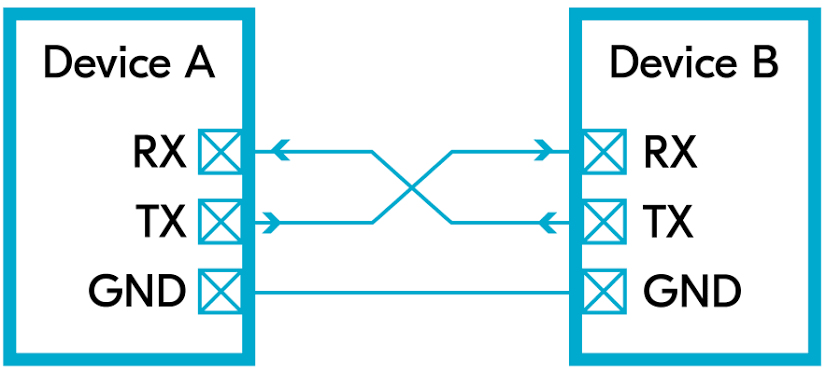
The wiring is crossed: the TX of one device goes to the RX of the other, and vice versa.
The two GND pins are tied together so both sides share the same voltage reference.
UART is asynchronous, which means it doesn’t carry its own clock.
Therefore, both parties communicating must agree on a common clock speed before sending any data, by choosing the baud rate, the number of bits sent per second.
They must also agree on the frame format:
- Data bits: usually 8
- Parity: an optional error-detection bit — N (none), E (even) or O (odd)
- Stop bits: how long the line stays high after the data, usually 1 bit period
Note that none of this is negotiated over the wire, each side must be configured manually beforehand. That’s UART’s best feature, since a chip can talk as soon as a few registers are written, with no driver or stack. It’s also its worst: a mismatch gives you garbage, never an error.
Communication
The default state of TX is high (logical 1) for IDLE.
Here is the process for sending a byte:
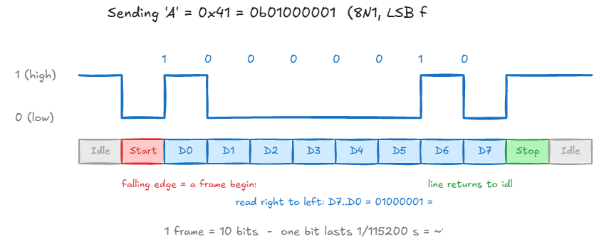
- Start bit: the line drops to 0, telling the receiver a frame begins.
- Data: the 8 bits, least significant bit first.
- Stop bit: the line goes back to 1.
The receiver never detects the end of a frame, it counts: after the start bit, it samples the line once per bit period, eight times, which is exactly why a wrong baud rate produces garbage instead of an error.
Therefore, the stop bit is not an end marker, it simply returns the line to idle.
UART vs Mini UART
The BCM2837 has two UARTs: a full ARM PL011, and a stripped-down “mini UART” living in an auxiliary block. On the Pi 3, the PL011 is wired to the Bluetooth chip by default, so the pins on the header go to the mini UART.
It buffers bytes in two small 8-byte FIFOs, one per direction. And its baud rate is derived from the VideoCore’s core clock, which will come back to annoy us later.
Here is a detailed list of the main differences:
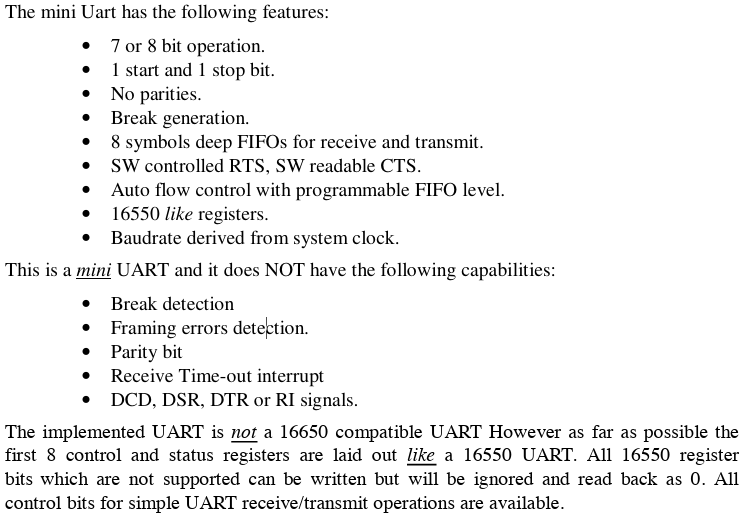
We will be using the 115200/8N1 standard for our Mini UART: 115200 baud, 8 data bits, no parity, 1 stop bit.
The mini UART is deliberately minimal: 8N1 is not really a choice, since it only supports one stop bit and no parity, and it detects no errors at all.
Finding the addresses
Let’s start with the GPIO controller’s registers, which show the whole method:
enum {
    PERIPHERAL_BASE_ADDR = 0x3F000000,
    GPFSEL0         = PERIPHERAL_BASE_ADDR + 0x200000,
    GPPUD           = PERIPHERAL_BASE_ADDR + 0x200094,
    GPPUDCLK0       = PERIPHERAL_BASE_ADDR + 0x200098
};
The datasheet lists every register at an address starting with 0x7E. Those are bus addresses, seen from the VideoCore. The ARM sees the same peripherals at 0x3F… .
So GPFSEL0, listed at 0x7E200000, is 0x3F200000 for us.
The MMU is off, so these are the addresses the CPU uses directly.
MMIO
Addresses in hand, we still need a way to read and write their values.
On the BCM2837, that is done through a mechanism called Memory-Mapped I/O (MMIO).
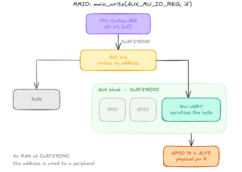
A CPU reaches the outside world the same way it reaches RAM: by putting an address on the bus. So instead of a special instruction per peripheral, the SoC gives each peripheral a range of addresses. That’s MMIO: peripheral registers are driven with ordinary loads and stores.
Writing to 0x3F215040 (AUX_MU_IO_REG) sends a byte to the mini UART and the CPU never knows the difference.
The bus looks at the address and routes the access to the UART instead of RAM, as there is no RAM there at all.
void mmio_write(unsigned long addr, unsigned int val)
{
  *(volatile unsigned int *)addr = val;
}

unsigned int mmio_read(unsigned long addr)
{
  return *(volatile unsigned int *) addr;
}
These two functions are the only ones touching hardware in our code, and as you can see they are pretty easy :)
The keyword that matters is volatile which it tells the compiler that every access it must not cache, merge or drop reads and writes.
Without it, the compiler could read the UART status once and reuse the result for another use case for example.
GPIO
Our building blocks are ready. Let’s put them to work on the GPIO first, because nothing leaves the chip until both pins are wired to the UART !
ALT5
Our SoCs can have a lot of peripherals (UART, SPI, I2C, …), but only have a limited number of pins.
That is why it uses multiplexing: each pin is connected to multiple devices.
Each one can be wired to several peripherals, and a switch picks which one drives it
The registers responsible for this are GPFSEL(0-5).
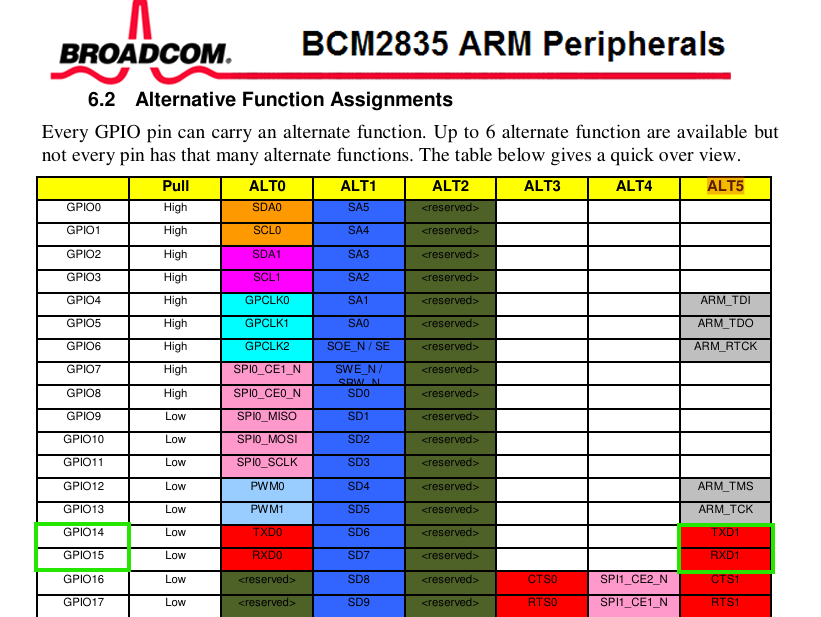
Our Mini UART uses ALT5 so as we need to interact with TXD1 and RXD1, we will be using pins 14 and 15.
Pin 14 will be used to send data and Pin 15 to receive data.
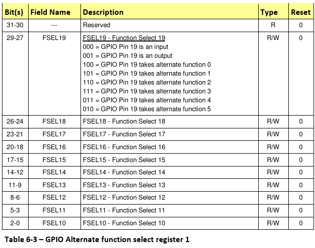
We can guess two things thanks to the documentation:
The first is that the size for each field is 3 bits, as each FSEL covers 3 bits and 9 modes.
The second is that each GPFSEL covers 10 pins (10 FSEL per table).
Therefore, as we are going to use GPFSEL1 for both pin 14 and 15, and FSEL14/15 with 010 to select ALT5.
Our goal is to therefore to set bits 12-14 to 010 without touching the 29 others.
We will have to do some arithmetics here !
Let’s take the value for our GPFSEL1 value:
FSEL :          19  18  17  16  15  14  13  12  11  10
                                     ↓
val :           010 110 111 110 011 011 001 010 101 110

1. Mask         000 000 000 000 000 111 000 000 000 000    7 << 12
2. Invert       111 111 111 111 111 000 111 111 111 111    ~(7 << 12)
3. AND          010 110 111 110 011 000 001 010 101 110    val & ~(7 << 12)
4. Value        000 000 000 000 000 010 000 000 000 000    2 << 12
5. OR           010 110 111 110 011 010 001 010 101 110    val | (2 << 12)
Here’s our final calculation chain:
void gpio_set_alt5(unsigned int pin)
{
  unsigned int reg = GPFSEL0 + (pin/10)*4;
  unsigned int shift = (pin % 10) *3;
  unsigned int val = mmio_read(reg);
  val = val & ~(7 << shift);
  val = val | (GPIO_FUNCTION_ALT5 << shift);
  mmio_write(reg,val);
}
This step is not optional: until the switch is flipped, the UART can be configured perfectly and still send its bits nowhere, because they never reach the physical pin.
Pull
One thing we still haven’t dealt with are the pull resistors.
A pin configured as an input and left unconnected has no defined state: its voltage floats with ambient electromagnetic interference, so reading it returns random values. The solution is small internal resistors that pull the pin to a known level, towards 3.3V for a 1, or GND for a 0.
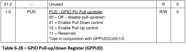
GPIO Pull-up/down Register (GPPUD) is simple: only its two lowest bits matter.
We have three states:
enum {
    PULL_NONE = 0,
    PULL_DOWN = 1,
    PULL_UP   = 2
};
Our PULL_* enum mirrors these values.
The key detail is the note at the bottom: “Use in conjunction with GPPUDCLK0/1/2”.
Indeed GPPUD tells what to do and GPPUDCLK0 tells who does it.
The datasheet gives the sequence to apply it:
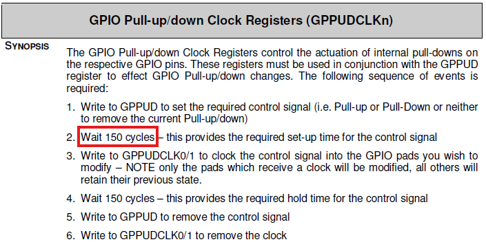
Notice the “wait 150 cycles”.
C has no notion of a cycle, so we cannot write that directly. And the datasheet does not say whether 150 is a minimum or an exact value.
This is where I got stuck for a while.
Searching GitHub for GPPUD "150 cycles" led me to this library, which drives the same chip: janne/bcm2835
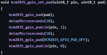
As we can see it waits for 10 µs between each step.
At a 250 MHz system clock, that is 2500 cycles. Far more than 150 !
Makes sense: the datasheet calls these waits set-up and hold times, which are minimum durations by nature. Waiting longer is fine.
Let’s try to be more precise though and settle around 150 cycles by calculating the right time to wait.
150 / 250 000 000 = 0.6 µsSo we need to wait at least 0.6 µs.
To measure that, the BCM2837 has a System Timer whose CLO register counts up by one every microsecond. The datasheet lists it at 0x7E003004, so 0x3F003004 for us:
enum {
    SYSTMR_CLO = PERIPHERAL_BASE_ADDR + 0x3004
};
We read the counter once, then keep reading until it has moved forward enough.
void delay_us(unsigned int us)
{
    unsigned int start = mmio_read(SYSTMR_CLO);
    while (mmio_read(SYSTMR_CLO) - start < us);
}
The counter only counts whole microseconds, so we cannot wait exactly 0.6 µs. And one tick is not enough: if the counter was about to tick when we started, we would barely wait at all.
So we call delay_us(2), which guarantees at least a full microsecond.
There is actually a difference here for the Raspberry Pi 4 this whole dance is gone: a single register, GPPUPPDN0, holds a readable 2-bit field per pin, so setting a pull is one write instead of a six-step sequence with timing constraints.
Unlike GPFSEL, we write GPPUDCLK0 directly without reading it first:
// Write No Pull to GPPUD
mmio_write(GPPUD,PULL_NONE);
delay_us(2);

//Set pin 14 and 15 in GPPUDCLK0
mmio_write(GPPUDCLK0, (1 << 14) | (1 << 15));
delay_us(2);
Now that the values are stored in pins 14 and 15, we need to clean everything and set back both registers:
//Clean both registers
mmio_write(GPPUD, PULL_NONE);
mmio_write(GPPUDCLK0, 0);
You may be wondering why do we set them back to 0 if the goal of the function is to set them to 1 ?GPPUDCLK0 does not hold the pull state: it is a trigger.
Therefore setting it to 1 for a few microseconds sends the information to our SoC to disable pull but once the cycle is done, we can set it back to zero without it to change the state back.
UART
The most complex part is done: our 2 pins lead straight to our mini UART.
Now the final part is to use these GPIO functions in the right order to set up and orchestrate our UART.
The mini UART has its own set of registers, all packed in one auxiliary block:
enum {
    AUX_BASE        = PERIPHERAL_BASE_ADDR + 0x215000,
    AUX_ENABLES     = AUX_BASE + 4,
    AUX_MU_IO_REG   = AUX_BASE + 64,
    AUX_MU_IER_REG  = AUX_BASE + 68,
    AUX_MU_IIR_REG  = AUX_BASE + 72,
    AUX_MU_LCR_REG  = AUX_BASE + 76,
    AUX_MU_MCR_REG  = AUX_BASE + 80,
    AUX_MU_LSR_REG  = AUX_BASE + 84,
    AUX_MU_CNTL_REG = AUX_BASE + 96,
    AUX_MU_BAUD_REG = AUX_BASE + 104,
    AUX_UART_CLOCK = 250000000,
    UART_BAUD_RATE      = 115200,
    AUX_MU_BAUD_VAL = (AUX_UART_CLOCK / (UART_BAUD_RATE * 8)) - 1
};
AUX_BASE points to the start of the auxiliary peripheral block, which the BCM2837 shares between the mini UART and two SPI masters, hence the AUX_ prefix on everything.
Everything else is an offset inside it, and they fall into three groups.
- Gatekeeping:
AUX_ENABLESis the master switch for the whole block, until its bit is set, the other registers cannot be read or written. - Setup:
AUX_MU_LCR_REG: frame formatAUX_MU_BAUD_REG: speedAUX_MU_CNTL_REG: switches TX and RX onAUX_MU_IER_REG: enables interruptsAUX_MU_IIR_REG: identifies the interrupt + allows to clear our I/O FIFOsAUX_MU_MCR_REG: hardware flow control (RTS line)
The last 3 registers will be turned off as we use polling instead of interruptions.
- Traffic:
AUX_MU_LSR_REG: tells us whether the transmitter is free or a byte has arrivedAUX_MU_IO_REG: where bytes actually go in and out.
AUX_UART_CLOCK: It’s the VideoCore’s core clock, which the firmware may scale at runtime and drag our baud rate with it. That’s why we pin it at 250 MHz inconfig.txtlater.
The mini UART divides down to produce the baud rate, found with the following:

The 8 comes from the mini UART sampling each bit eight times.
Our formula for the register:
AUX_MU_BAUD_VAL = (AUX_UART_CLOCK / (UART_BAUD_RATE * 8)) - 1At 250 MHz targeting 115200 baud, that gives us around 270.
Note:
A wrong peripheral base address gives you silence as the writes land nowhere at all.
A wrong clock gives you garbage characters, because the UART works perfectly and only the timing is off.
Knowing which of the two you are looking at tells you immediately where to start debugging.
Init
To begin, we need a startup routine. It is mostly a list of many register writes.
Each register was introduced above, so the comments speak for themselves:
void uart_init(void)
{
  //Select GPIO ALT5 Function
  gpio_set_alt5(14);
  gpio_set_alt5(15);

  //Disable Pull Resistors
  disable_pull();

  //Enable Mini UART Auxiliaries
  mmio_write(AUX_ENABLES, 1);

  //set TX and RX down for init
  mmio_write(AUX_MU_CNTL_REG, 0);

  //Set data format to 8 bit-mode
  mmio_write(AUX_MU_LCR_REG, 3);

  //Setting Baud rate
  mmio_write(AUX_MU_BAUD_REG, AUX_MU_BAUD_VAL);

  //Making sure IER and MCR are set to zero
  mmio_write(AUX_MU_MCR_REG, 0);
  mmio_write(AUX_MU_IER_REG, 0);

  //Clearing receive and transmit FIFOs
  mmio_write(AUX_MU_IIR_REG, 2 | 4);

  //Enable TX and RX
  mmio_write(AUX_MU_CNTL_REG, 3);

}
What the code does not show is why the order matters:
- GPIO first: The datasheet asks for the pins to be routed before the UART is enabled.
Otherwise, the RX line reads low, which the mini UART reads as an endless stream of start bits and0x00bytes. AUX_ENABLES: Essential as all mini UART registers cannot be written without itCNTL: We switch TX and RX off before touching the configuration, and back on only once everything is set.
A good habit worth mentioning: set every register you rely on, even when you expect it to already hold the right value.
Other code runs before ours at boot: the firmware may have touched the UART, so we never assume a register’s state. That is why IER and MCR are explicitly cleared.
Note: you’ll see 0xC6 written to IIR in many tutorials; bits 7:6 are read-only, so 6 still works and is easier.
Sending data
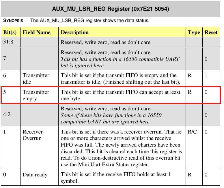
The first line is the whole idea of polling: we keep reading LSR until bit 5 says the transmit FIFO has room for at least one byte.
We can use a & mask to isolate that single bit (detailed it in ALT5 section), and the loop spins as long as it is 0.
Only then, we can write our byte to IO_REG, and the mini UART shifts on the wire.
We can now write our function in order to write each character of the string one by one:
void uart_putc(char c)
{
  //Waiting for FIFO to accept at least 1 byte
  while (!(mmio_read(AUX_MU_LSR_REG) & (1 << 5)));

  //Write char
  mmio_write(AUX_MU_IO_REG, c);
}
void uart_puts(const char *s)
{
int i = 0;
while(s[i])
{
if(s[i]=='\n')
uart_putc('\r');
uart_putc(s[i]);
i++;
}
}Good old puts function, been repeating it so much when learning to code i’ve been dreaming of it some nights ! Maybe not the only one :))
Note: Terminals expect \r\n: a bare \n moves down without going back to column 0, so we add the \r ourselves.
Linking it all together
Boot code
Before main() can run, a few lines of assembly are needed to prepare the ground.
We won’t dive into it but boot.S does three main things:
- Set up a stack, as C needs one for its first function call
- Zero sections such as
.bss, C expects them to be filled with zero for global variables - Call
main()
C Files
Then it’s time to create our main:
#include "io.h"

void main(void)
{
  uart_init();
  uart_puts("Hello world\n");
  while(1);
}
Note the infinite loop at the end: there is no operating system to return to. If main() returned, execution would fall back into boot.S, and whatever sits in memory after the call would run next. A kernel never exits: it is the last link in the boot chain.
The linker script places boot.S first, at 0x80000, which is where the firmware jumps to our kernel8.img. Then we have the Makefile to automate the build.
Both files were borrowed from sypstraw’s rpi4os project.
Build and Run
QEMU
If you want to run it with QEMU, make sure that you have qemu-system-aarch64 and the aarch64-linux-gnu-gcc cross-compiler.
Then you simply need to clone the repository, build it with make and run the following command:
qemu-system-aarch64 -M raspi3b -kernel build/kernel8.img -serial null -serial stdio -display noneNote that the -serial null -serial stdio pair matters as QEMU maps its first serial port to the PL011 and the second one to the mini UART. We discard the first and plug the second into our terminal.
However, keep in mind that QEMU is great to check the logic, but it does not validate everything.
It has no real pins, so a wrong GPIO setup goes unnoticed.
It also forwards bytes without real timing, so a wrong baud rate does not show up either.
Only the real board tests those !
Raspberry Pi 3B+
First, make sure your pins are plugged from your FT232 controller as follows:
- FT232 TXD → Pin 10 (RXD)
- FT232 RXD → Pin 8 (TXD)
- GND → Pin 6
The Pi’s boot ROM looks for a FAT32 partition.
On it, we need the files that are provided inside the folder firmware/:
- bootcode.bin: Second Stage bootloader, starts SDRAM and loads
start.elf - config.txt: Kernel settings used by
start.elf - fixup.dat: Sets up the memory split between the GPU and the ARM. used by
start.elf - start.elf: VideoCore firmware, loads
kernel8.imginto RAM
Build the kernel first with make, which drops it in build/kernel8.img.
Then find your SD card’s boot partition (the vfat one, usually /dev/mmcblk0p1 or /dev/sdX1):
lsblk -fMount it, clear it and copy everything:
sudo mkdir -p /mnt/sd
sudo mount /dev/mmcblk0p1 /mnt/sd
sudo rm -rf /mnt/sd/*
sudo cp firmware/* build/kernel8.img /mnt/sd/
Then flush and unmount before pulling the card out:
sync
sudo umount /mnt/sd
Now it’s time to test it in real conditions!
Insert the SD card in the Pi.
Before plugging the power supply of your Pi, launch a UART session on your machine:
picocom -b 115200 /dev/ttyUSB0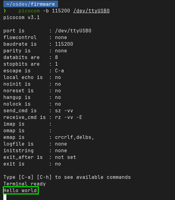
Let’s goooo !
This is the longest “Hello World” I’ve ever written :))
Wrapping up
This was my first blogpost and project of OS development.
I hope you learned things on the road and that it made you want to dive into Bare Metal programming !